Start from parts with lowest profile/height and finish with jacks and footswitches.
First thing to solder are the SMT parts if needed: 2 x ferrite beads and 2 x SO-8 ICs.
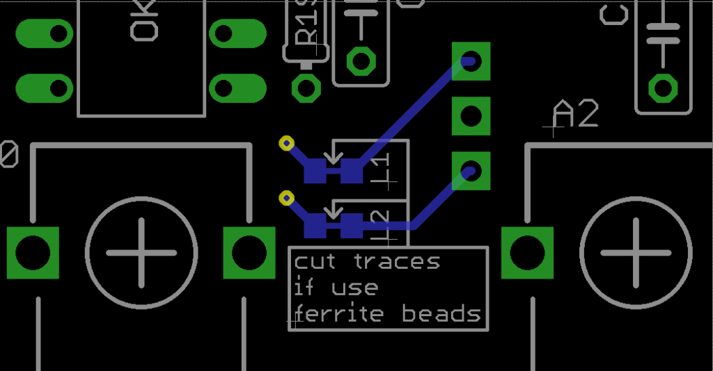
MIDI ferrite beads
MIDI circuit has two small ferrite beads in 0603 package labeled L1 and L2 on PCB, these tiny little parts are needed to prevent noise in MIDI circuit. Noise only happens when a MIDI message is received and only is heard while communication is happening (so in a short amount of time). If you want to use the ferrite beads cut the traces as indicated on PCB silkscreen and solder the ferrite beads.
External SRAM and a lot of considerations about
External SRAM comes in a SO-8 SMT package but you may need it or not depending on your purposes.
Why you need or not more SRAM?
Short answer: for longer delay times
Long answer: natively adau1452 can allocate delay to data memory and program memory. Data memory is approx 40k words while program memory is 8k words. So how much delay can we get in this configuration?
delay time in milliseconds = (1/sample rate) * 49184 = 1024 ms @ 48khz
This is a theoretical calculation since almost every DSP operation like filtering makes use of some delay, altough very small, and really depends on your algorithm.
Delay is used for many applications in audio processing like reverb, pitch shifting and…delay effect of course!
External SRAM adds 32k words for delay operation, so using the above formula we get around 680 ms of delay more for a total of 1.7 seconds.
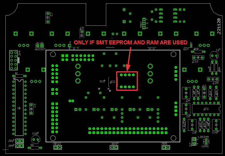
SMT EEPROM is used only if external SRAM is used.
In the end, if using external RAM:
- Solder SO-8 23LC1024 to IC3 and SO-8 25AA1024 to IC2
- Solder 2 x female header (1×4) on main PCB and 2 x male header (1×4) on DSP board
If not using external RAM:
- Solder DIP-8 25AA1024 on the DSP board
Solder all the other THT parts
- Solder resistors top and bottom side of the PCB
- Solder diodes top and bottom
- Solder ceramic caps and metal film caps top and bottom
- Solder transistors top and bottom
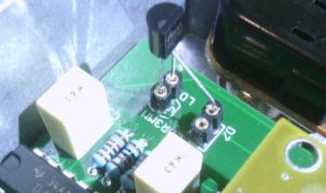
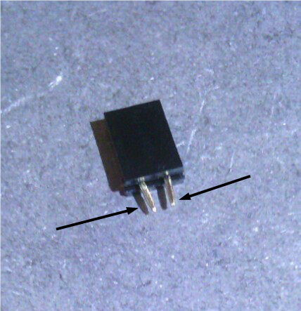
On PCB dated 221120 a BS170 mosfet transister must be soldered in place of LDR1 and D7, solder as showed in the following picture. Basically external legs of the BS170 go to LDR1 and central leg goes to A of D7 (don’t mind the sockets in the picture):
- Solder ICs and/or IC sockets
All ICs can be direct soldered without sockets but it’s suggested to use DIP-28 socket for U1 in case you want to remove and reprogram it.
- Solder female headers:
The 1×2 pads have a pitch which is not exactly 2.54mm so you’ll need to bend the pins of header a bit to make it fit inside the holes:
- Solder male headers JP5 and JP4 silkscreen side
- Solder potentiometers on the silkscreen side:
- Solder wires on the silkscreen side:
- Place LEDs and toggle switches on PCB silkscreen side, don’t solder them yet. Take the drilled enclosure and fit in the assemblied PCB, adjust LEDs and toggle switches so they fit inside the enclosure. Once everything looks good solder LEDs and toggle switches.
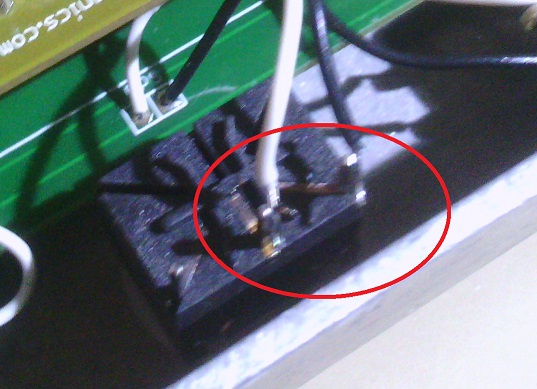
- Mount jacks and footswitch on enclosure and solder to the wires mounted earlier. MP13 and MP5 don’t have a polarity. BPS must be solder to the common and N.O (normally open) terminals of the 3 pin footswitch, no polarity either:
- The mini jack DC has 2 pins. If you use a negative center PSU (which is standard in guitar pedal world) connect short pin to ground and long pin to +9V pads
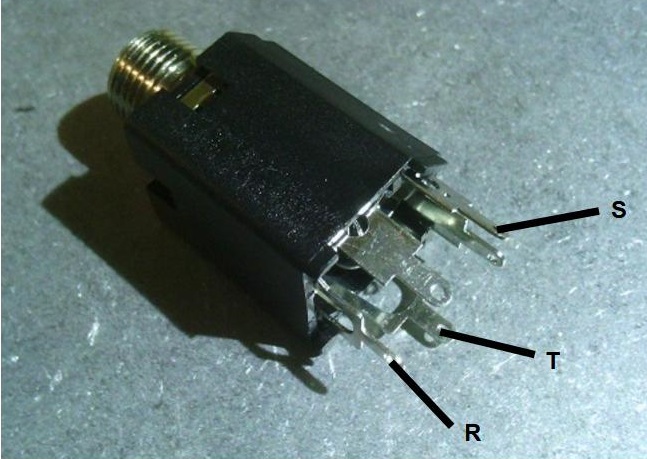
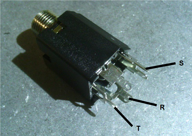
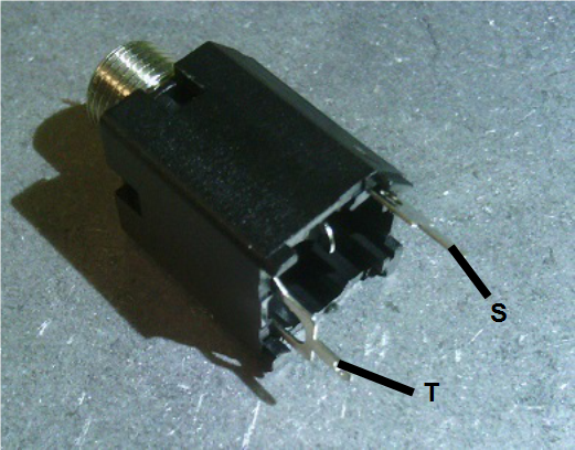
- 6.35mm jacks are either TS and TRS. TS are used for IN0, OUT0 and OUT1. TRS are for EXP in and MIDI in.
MIDI in:
IN0, IN1, OUT1 jack:
EXP jack: